Checking out Large Thickness Interconnect Engineering: Developments, Software, and also Upcoming Styles
Inside the sphere regarding electronic digital producing, the particular unremitting search for more compact, more quickly, plus more potent gadgets provides generated the particular advancement of varied interconnect technology. Between these kinds of, Large Thickness Interconnect (HDI) stands apart being a important advancement circuit card assembly includes revolutionized the style and also creation regarding published routine panels (PCBs). HDI engineering permits the particular integration regarding a lot more parts directly into more compact places, increasing efficiency, trustworthiness, and also features. In this post, we all look into the particular ins and outs regarding HDI engineering, the software around market sectors, latest developments, and also upcoming styles.
Comprehending Large Thickness Interconnect (HDI) Engineering:
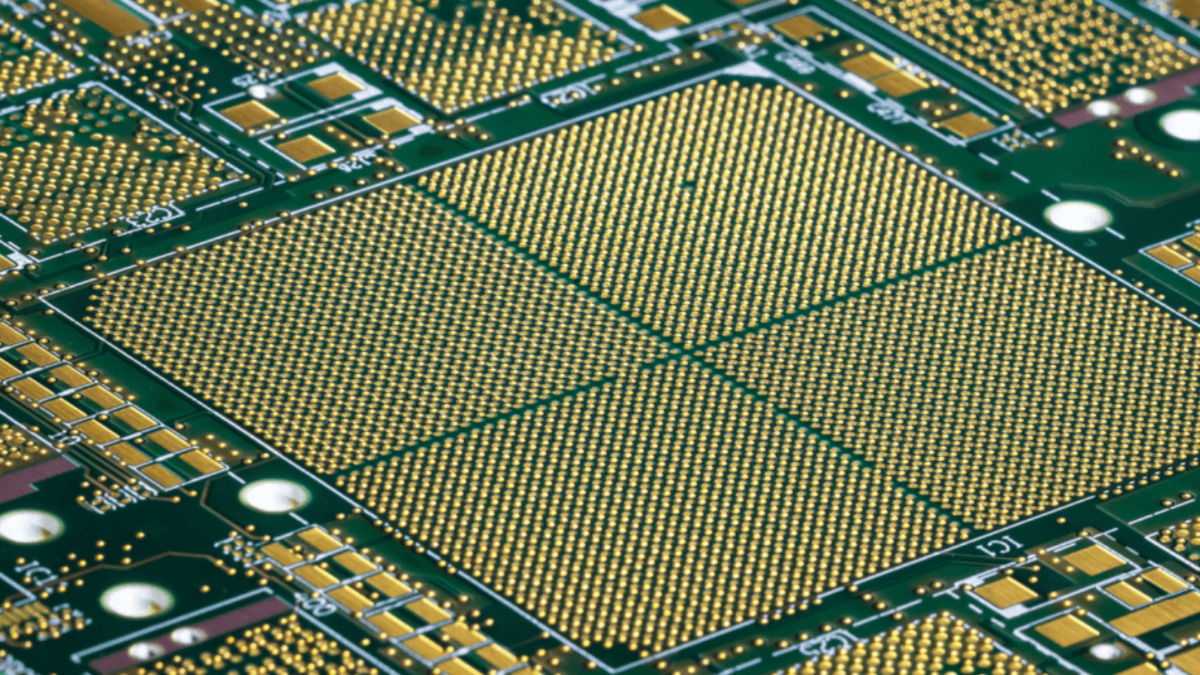
HDI identifies any engineering that enables for your manufacture regarding PCBs together with increased routine densities and also better traces and also places as compared to standard strategies. This kind of progression inside PCB layout requires the use regarding microvias, great traces and also places, and also superior level stacking ways to attain better features and also miniaturization. As opposed to standard PCBs, which usually largely employ through-hole vias and also greater track widths, HDI panels use numerous tiers regarding densely crammed footprints interconnected by means of microvias, permitting considerable area financial savings and also improved upon sign strength.
Advancement and also Developments:
The particular advancement regarding HDI engineering may be followed returning to the particular improving requirement regarding more compact plus more light gadgets, specifically inside market sectors for instance electronic devices, telecom, and also health-related gadgets. Since gadgets started to be smaller sized, standard PCB producing strategies fought to help keep rate with all the dependence on increased routine densities and also improved upon efficiency.
One of many important developments inside HDI engineering could be the using laserlight drilling regarding producing microvias. Laserlight drilling presents unrivaled accurate and also handle, enabling the particular generation regarding more compact dimension vias together with increased factor proportions. In addition, developments inside components research have got generated the particular advancement regarding high-performance substrates and also laminates able to assisting the particular great characteristics and also high-density course-plotting necessary simply by HDI models.
Software Around Market sectors:
The particular adaptability regarding HDI engineering provides caused it to be vital around many market sectors. Inside electronic devices, HDI PCBs permit the particular advancement regarding ultra-thin cell phones, capsules, and also wearable gadgets with out reducing about efficiency. The particular car market employs HDI engineering to be able to combine intricate electronic digital methods directly into autos, which includes superior driver-assistance methods (ADAS) and also infotainment methods.
Additionally, HDI engineering takes on an essential function inside aerospace and also security software, in which trustworthiness and also miniaturization are usually essential. Space-constrained health-related gadgets, for instance pacemakers and also implantable receptors, take advantage of the lightweight kind aspect and also large trustworthiness made available from HDI PCBs. The particular professional market furthermore utilizes HDI engineering regarding automation, robotics, and also IoT gadgets, in which area marketing and also robustness are usually vital.
Latest Developments and also Innovative developments:
Lately, the particular progression regarding HDI engineering continues to be propelled simply by innovative developments inside producing techniques, components, and also layout equipment. Three-dimensional (3D) stamping strategies have got come about being a encouraging method regarding creating intricate HDI constructions together with lowered direct instances and also charges. Component producing permits the particular generation regarding complex geometries and also custom-made models, checking fresh opportunities regarding next-generation gadgets.
Moreover, the particular integration regarding man-made brains (AI) and also equipment studying algorithms in to the PCB layout method provides triggerred the particular marketing regarding HDI styles regarding improved upon sign strength, winter supervision, and also trustworthiness. AI-driven layout equipment examine great numbers of info to spot ideal course-plotting adjustments, level stackups, and also by means of positionings, increasing the particular advancement routine and also increasing functionality.
Upcoming Styles and also View:
Seeking in advance, the long run regarding HDI engineering will be positiioned regarding continuing progress and also advancement. With all the arrival regarding 5G sites, World wide web regarding Items (IoT) gadgets, and also side calculating software, the particular requirement regarding lightweight but potent electronic digital methods will simply accentuate. HDI engineering will be anticipated to enjoy any crucial function inside achieving these kinds of calls for simply by permitting the particular advancement regarding high-performance, miniaturized PCBs to get a different selection of software.
Additionally, the particular convergence regarding HDI engineering together with some other growing styles, for instance adaptable and also stretchable electronic devices, bioelectronics, and also quantum calculating, keeps assure regarding revolutionary developments inside electronic devices producing. Adaptable HDI substrates can revolutionize wearable electronic devices and also conformal health-related gadgets, although quantum-inspired course-plotting algorithms can boost interconnects inside next-generation calculating methods.
In summary, Large Thickness Interconnect (HDI) engineering symbolizes any building block regarding modern day electronic devices producing, permitting the particular advancement regarding more compact, more quickly, plus more trustworthy gadgets around market sectors. Together with continuous developments inside components, producing techniques, and also layout strategies, HDI engineering will be positiioned to carry on traveling advancement and also surrounding the long run regarding electronic devices regarding years into the future.
Leave a Comment